Low
Noise, Low Current
Band
Gap Regulator Design
Tutorial
Kevin Aylward
B.Sc.
https://www.kevinaylward.co.uk
05/12/2025
Abstract
This
tutorial details how to design a “state of the art” band gap regulator. It
assumes that the reader already has a reasonable understanding of analog
design. The purpose of this tutorial is only to present knowledge that may not
be known in general.
Furthermore,
in contrast to the bulk of formal academic papers, the approach here is to use
the absolute minimum of mathematics, and use simulation to arrive at the
optimum results.
In
the actual real professional engineering world, it’s just a fact of reality,
that the vast majority of analog ASIC design is performed entirely in the
virtual simulation universe of Cadence. Pages of highbrow, complicated
equations so often used in papers, are fundamentally useless in real actual
analog design and achieve nothing.
What
is important, is understanding the global principles, and using simulation to
do all of the doggy work.
The
key design specifications of this tutorial are to achieve low noise with a
current vastly lower than any conventional classical topology. Specifically
this example design approach achieves:
Flat-band noise:
40nv/√hz
Current: 70ua
Which
can be compared to commercial products such as:
LTC6655
Flat-band noise:
35nv/√hz
Current: 5ma
Basic Topology
The
fundamental principle of achieving a voltage that is independent of
temperature, is to add two independent voltages, one which has a positive
temperature coefficient with one that has a negative coefficient. This is
achieved by using a diode and a PTAT.
A
diode generates a nominal 0.7V with notional linear temperature coefficient of ~
-2mv/deg .
A
standard PTAT generator of the established literature generates a nominal 50mV
with a linear temperature coefficient of ~160uv/deg
This
means that in order for the VPTAT temperature coefficient to cancel out the
temperature coefficient of the diode , a gain of around 12 must be applied to
the VPAT voltage
This “noise gain” is the fundamental reason why standard Band Gap
regulators are relatively noisy.
This
system is illustrated by this example:
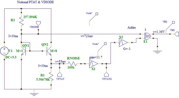
Figure
1 - PTAT Diode Band Gap System
Schematic

Figure
2 - Band Gap Output Voltage
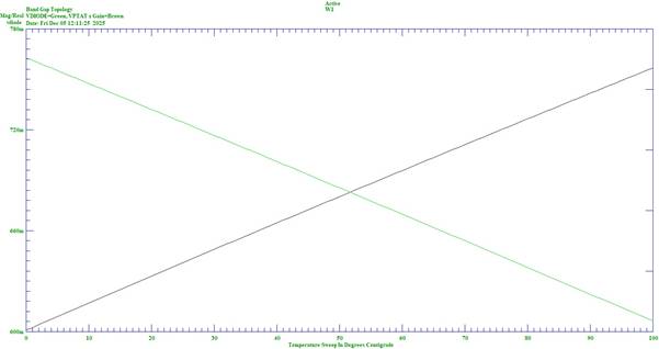
Figure
3 - VPTAT & VDiode

Figure
4 - VPAT & Diode Noise – 475 nV/√hz
The
apparent Chicken & Egg issue shown here, is that there is a constant supply
powering this system, which, is notionally supposed to provide the constant
voltage in the first place. This is only for the purposes to illustrate the
principle. In the final design, the power for the blocks is provided by the
output of the regulator itself, with an appropriate start-up circuit.
Improvements 1
Improvements
to this system can be made as follows:
1
Increase
the ratio of the transistor area to increases the temperature coefficient
2
Change
the ratio of the currents in the transistors to increase the temperature
coefficient
3
Stack
two PTAT cells on top of each other to increase the temperature coefficient
These
modifications can be made without changing the supply current, and result in
the gain of the PTAT being reduced, thereby reducing the output noise, as
follows:
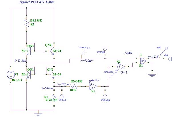
Figure
5 - PTAT Diode Band Gap System
Schematic Modified

Figure
6 - Band Gap Output Voltage
Modified

Figure
7 - VPTAT & VDiode Modified
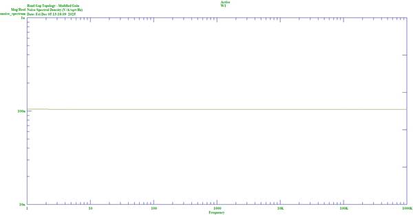
Figure
8 - VPAT & Diode Noise – 104 nV/√hz
The modified design only requires a gain of 2.4
compared to 11.7, resulting in a noise reduction from 475nv/ √hz to 104nv/ √hz.
Improvements
2
Further improvement can be made by adding the
voltages of several cells. This takes advantage of the principle that doubling
the voltage by adding cells, only multiplies the noise by √2. This is
illustrated as followers:

Figure
9 – Schematic Doubled VPTAT

Figure
10 - 2xVPAT & Diode - Band Gap
Output Voltage Modified 2
Figure
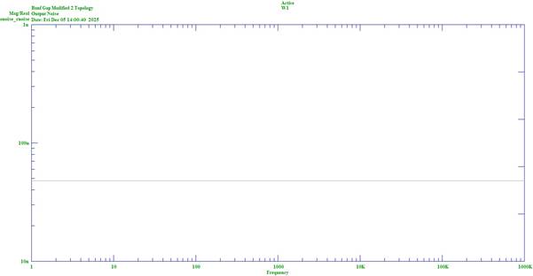
11 – 2xVPAT & Diode - Modified 2 Noise= 48 nV/√hz
The gain for the topology of adding of the cell
voltages is 1.18, around ½ of the single cell, which results in the noise being
further reduced to 48 nv/√hz.
It is noted that this is achieved by halving the
current of each cell so that the total current remains the same. This is to
ensure one is comparing apples with apples.
Improvement
3
An additional; improvement can be made to minimise
the noise when a nominal 1.23V is stepped up to a nominal voltage of say 2v5.
This is to again take advantage that doubling noise
voltages, only increases the noise by √2.
Two diodes can be used to double the nominal output
voltage, with additional stages of VPTAT added to compensate for the doubling
of the negative slope temperature coefficient.
An example is shown below.
Output voltage =2.48, with a required gain=1.15 and
noise=55nV/√hz
Figure
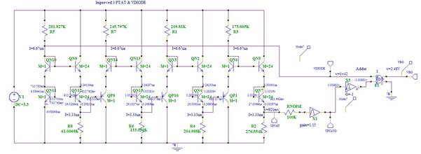
12 – Schematic Quadrupled VPTAT,
Doubled Diodes
Figure
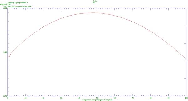
13 - Band Gap Output Voltage
Modified 3
Figure
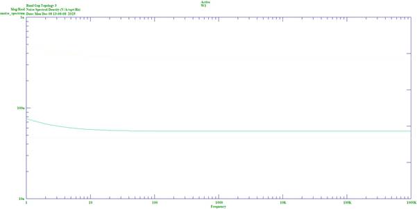
14 - 4xVPAT & 2xDiode Modified
2 - Noise = 55 nV/√hz
Improvement
4
In an actual design, there is a requirement to
connect some stages by current mirrors.
The noise of these notional mirrors can be reduced
by noting that they do not have to be strictly mirrors.
This allows the nominal DC gain of the mirror to
remain the same at say, 27 degrees, but have a reduced noise gain. For example:

Figure
15 - PTAT Current Mirror Normal and
Lower Noise

Figure
16 - PTAT Current Mirror Noise 32nv√hz & 29nv√hz
Full
Example
A complete design examples based on these principles
in included in the examples of the freeware Spice simulation software,
SuperSpice written by this author.
The design uses a differential amplifier with
feedback, with 2 Vbe junctions in the feedback forming the negative temperature
coefficient Vbe.
The power to the PTAT cells is derived from the
regulator output. Cascodes are used at the supply voltage side to ensure a high
PSRR.
A nominal process for the design is the XFAB XT018.
This process is a BICMOS process with complementary NPN/PNP bipolars, with no
RTS noise.
The summary of which is noted here:
IQ = 68ua
Vnoise = 38 nv/ √hz
PSRR DC = 90 dB
PSRR 10kHz to 100Mhz = 80 dB
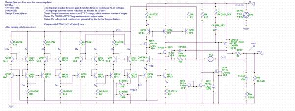
Figure
17 – Full Example Schematic

Figure
18 – Full Example Noise
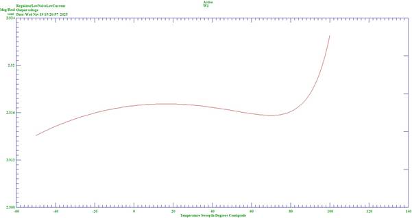
Figure
19 - Full Example VBG v Temperature
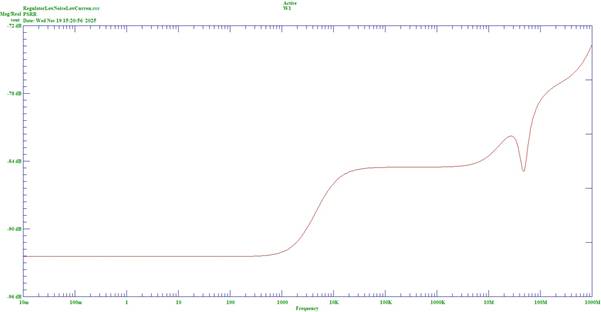
Figure
20 - Full Example AC PSRR
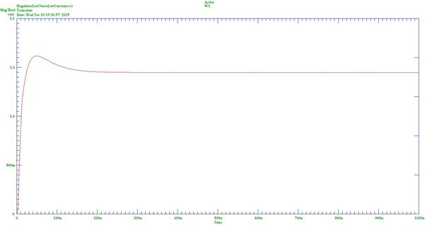
Figure
21 – Full Example Transient
Conclusion
A technique has been described that allows “state of
the art” regulators to be achieved. Specifically, achieving low noise at low
current.
Appendix
It is useful to note that a specific feature of the
SuperSpice software was used to set the resister values to achieve exact
notional values of current in the cell transistors. This was the “Device
Designer Feature”. This allowed the resistors to be told to adjust their value
to result in specific currents.
References:
Look them up !!!
Hint: Widlar…