Analogue Design
A Diode - CMOS Bandgap
Voltage Reference
Kevin Aylward B.Sc.
Overview
This paper describes the essentials of the design of a voltage reference using only the basic low beta pnp substrate diode connected transistor of a “pure” cmos process. It contrast to claims that to achieve low area, low low frequency noise and trimming accuracy, chopper amplifiers are required, this design approach yields relatively low, low frequency noise, good accuracy with the correct trimming procedure, and very high PSR.
Description
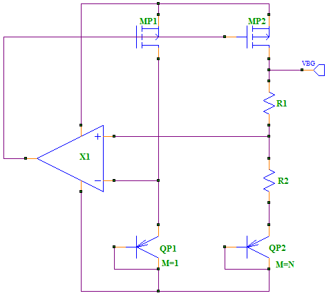
The standard pnp diode ptat bandgap topology is shown in Fig.1
Fig. 1 Standard diode based bandgap topology
Typically, quite a meal is made out of the amplifier X1. Usually a complete high impedance input, separate amplifier is designed quite distinct from the ptat generator itself. This is usually quite a complication, and is not necessary. An “all in a oner” topology is shown in Fig. 2.
Fig. 2 Integrated amplifier diode bandgap topology

This is, essentially, a folded
cascode amplifier combined with the ptat generator. The main gain being
achieved at the MN1/MP4 drains nodes, however it is a two gain stage topology.
The loop keeps all the currents ptat, and with the correct device sizes, all
voltages at QP1, QP2 and QP3 emitters equal. The effect of the folded cascode currents
on the diode currents, all comes out in the wash. The crucial bit is the bias
voltage of M1 and M2 being set by the same loop as the main ptat loop. One
minor pint, it turns out that there is an improvement is PSR if the cascode
currents are set to of the currents in MP1 and MP2 rather than
being equal.
To further improve PSR, cascode devices are added in the following example implementation shown in Fig. 3
Fig. 3 Example implementation of integrated amplifier
diode bandgap

Supply current is around 85 ua. Process is a 0.18u process but uses the 5V devices of that process.
A fundamental issue with bandgaps constructed with Mosfets, is the problem of process variations of the Mosfets, specifically, the mosfet’s threshold voltage, Vt.
It is often argued, as in Ref 1, that a nessesary solution to the problem of using only a one point temperature trim, is to use a chopper amplifier in order to eliminate the amplifier Vt offset. It is also claimed that the chopper is required to reduce 1/f noise to low enough levels. These claims are made on the assumption of being necessary if low die area is to be achieved.
A bipolar bandgap voltage reference is trimmed by determining the magic voltage at a set temperature, and trimming a resistor value until that voltage is achieved. This works for bipolars, because all errors essentially result in a rotate of the normal square law curve that resolves to the same curve when trimmed. This does not occur for mosfet Vt offsets. The magic voltage moves by the VPTAT amplification ratio times the offset (typically 6-8 times, but fixed and reproducible). The solution to this issue, is to simply monitor the differential voltage across the PNP emitters in a test mux mode in order to determine what the correction to the magic voltage is! Noting that any requirement to engage in trimming at all, means that one extra measurement has, essentially, no cost.
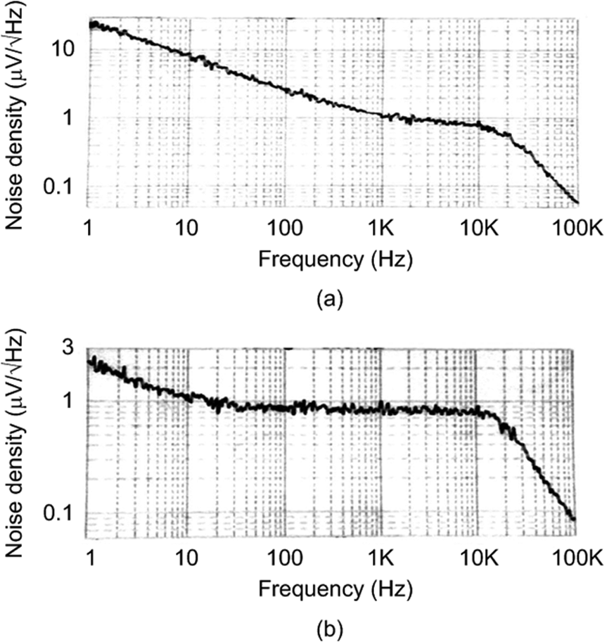
Ref 1 shows, for example, a reduction of 9 uv/sqrthz to 1uv/sqrthz at 10 Hz when its chopper is engaged, with an area of 0.12 mm2. However, the example in this paper also shows 1 uv/sqrthz at 10 Hz with an area of only around 0.02 mm2 ! Ok, its not quite apples with apples, the example here is just a basic un-buffered reference, but the point is that the 1/f noise is essentially due to the noise of the input Mosfets. Using “large” Mosfets reduces both the error and the noise. For this example, 3 sigma input offset will be of the order of < 1 mV, or around 6 mV maximum correction required to the magic voltage.
Results
Fig. 3
DC Temperature sweep over mosfet worst case corners

The worst case corners shows that the temperature set point is independent of global Vt variations, only the magic voltage changes.
Temperature variation is around 2.7 mv over -40 Degs. to 125 Degs., or equivalent to around +/-0.11%.
Fig. 4
DC Temperature sweep over +/- 4 mV Vt offset of MN2

Variation of Vt for MN2 shows the temperature set point is independent of Vt offset variations and that the “magic” bandgap voltage moves by around 7.2 mv/1 mv of Vt voffset.
Note that offsets may be around 20 mV- sqrt(LW) for typical processes, so for 20 um x 20 um x 8, expected 3 sigma offset would be around 1 mv, or around 7 mV shift in the magic voltage. Measuring this input offset is just a simple matter of adding one differential test mux input to the asic’s test system.
Fig. 5
Power Supply Rejection over Worst Case mosfet corners
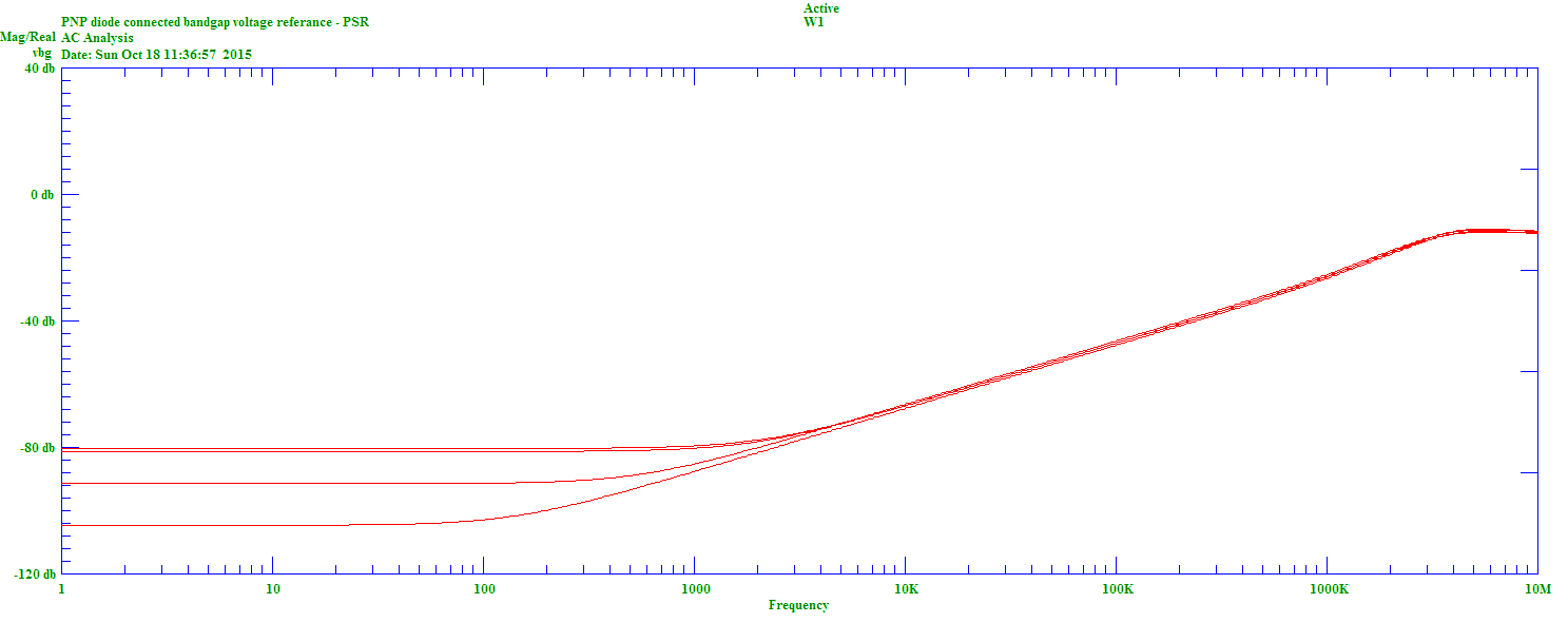
Nominal PSRR is around 90 dB, worst case around 80 dB.
Fig. 6
Noise

Nominal flat band noise is 160 nV/sqrthz. 10 Hz noise is 1 uV, 1 Hz noise is 3 uV
Fig. 7
Reference 1 With Chopper Noise and Without Chopper Noise
Summary
A PNP diode connected transistor bandgap voltage reference has been described that achieves equivalent low frequency noise and single temperature point calibrated error to that of a chopper amplified topology, and an order of magnitude lower flatband noise, with minimal die area.
References
1 - "A Single-Trim CMOS Bandgap Reference With a Inaccuracy of 0.15% From 40 C to 125 C" - Guang Ge, Cheng Zhang, Gian Hoogzaad, and Kofi A. A. Makinwa, Fellow, IEEE
2- “A Low Power
Differential CMOS Bandgap Reference” Todd L. Brooks, Alan L. Westwick
© Kevin Aylward 2015
All rights reserved
providing that this source is acknowledged.
Website last modified 23rd Oct 2015